PPPL will lead two CHIPS and Science Act projects
The U.S. Department of Energy (DOE) has awarded the Princeton Plasma Physics Laboratory (PPPL) two highly competitive Microelectronics Science Research Center projects. PPPL researchers will lead two collaborative projects involving national labs, as well as academic and industry partners. Princeton University researchers will act as deputy directors to the PPPL project directors.
Each award will provide $3 million per year and is expected to run for four years. The awards recognize PPPL’s expertise in the plasma processes that will continue to be critical to further developments in semiconductor manufacturing and the advanced materials that are needed to keep the U.S. globally competitive.
The DOE program leading to these awards originated from the CHIPS and Science Act of 2022. The DOE announced $179 million in total funding for three Microelectronics Science Research Centers (MSRCs). PPPL is part of two centers: the Co-design and Heterogeneous Integration in Microelectronics for Extreme Environments (CHIME) Center and the Extreme Lithography & Materials Innovation Center (ELMIC).
According to the DOE, the centers are formed as networks of 16 projects being led out of 10 national laboratories. These projects were selected by competitive peer review under the DOE Laboratory Announcement “Microelectronics Science Research Center Projects for Energy Efficiency and Extreme Environments.”
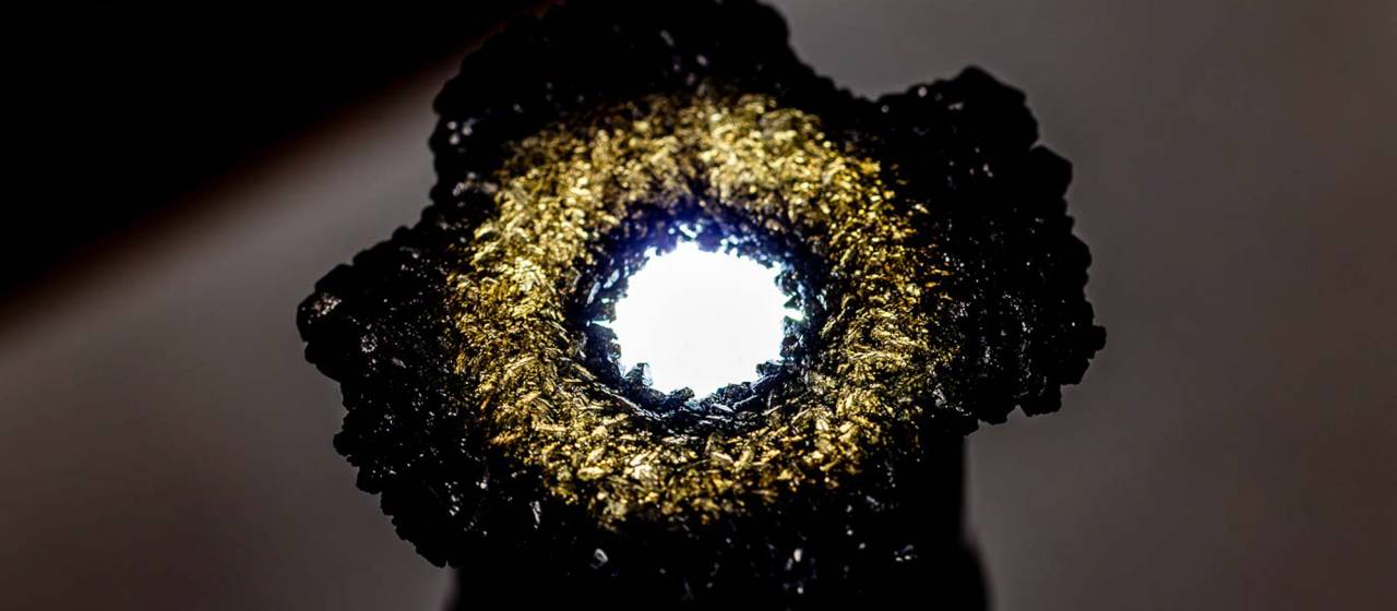
PPPL’s awards both went to projects focused on extreme environments because of their emphasis on plasma science. One of PPPL’s projects will investigate ways to make smaller, more capable microelectronics with 2D materials that are made using plasmas in high-temperature chambers. The other will look at the extreme properties of diamond material and how it can be used to make sensors and electronics that can handle harsh environments.
“These projects will provide a better understanding of how to craft the materials needed for next-generation semiconductors at the atomic scale,” said Emily Carter, the Gerhard R. Andlinger Professor in Energy and the Environment at Princeton University and associate laboratory director of applied materials and sustainability sciences (AMSS) at PPPL. “The outcomes of this research have the potential to profoundly influence multiple industries worldwide, reflecting the integral role microelectronics play in our daily lives.”
AMSS researchers are using their plasma expertise to develop new technologies in microelectronics, quantum sensing and sustainability. AMSS teams are already working with industry partners like Applied Materials, Lam Research and Samsung to develop new techniques for microchip fabrication and etching. The AMSS directorate also opened the Quantum Diamond Laboratory (QDL) at PPPL in March of 2024.
2D materials for next-generation semiconductors
Semiconductors are the foundation of the memory, storage and processing power used in commercial, industrial and military-grade devices. Unfortunately, scientists and engineers are reaching the limit on what can be done using the standard material — silicon — and existing processes, driving the need for further research.
Yevgeny Raitses, a managing principal research physicist at PPPL, will lead the project aimed at perfecting methods for incorporating 2D materials into 3D complex nanostructures. These materials are needed for next-generation microelectronics as researchers continue to push the envelope by fitting more features into ever-shrinking devices. Although 2D materials are mostly actually 3D, they are often made up of only a few layers of atoms. They are so thin that scientists call them 2D.
“Plasma is a critical component of nearly half of all semiconductor manufacturing processes,” said Raitses. ”We aim to create a science-based plasma-processing toolbox to enable the integration of 2D materials into next-generation semiconductor device manufacturing processes.”
The research team will also include researchers from Princeton University, the University of Michigan, the University of Houston, the University of California-Los Angeles (UCLA) and IBM Research’s Thomas J. Watson Research Center.
Diamond sensors for extreme environments
Alastair Stacey, a managing principal research physicist at PPPL and a professor of physics at the Royal Melbourne Institute of Technology (RMIT), will spearhead a second project to research ways to make highly resilient sensors out of diamond.
“There are a set of really extreme environments that most electronics can’t survive and that diamond might be able to do well in,” said Stacey, who is the head of PPPL’s quantum materials and devices and the QDL.
Sensors and electronics used in space, for example, sometimes need to withstand bombardment by potentially problematic particles, such as high-energy ions. Those used inside nuclear or fusion reactors and rocket thrusters need to tolerate high-energy particles and radiation, as well as immense heat, without breaking down. “Diamond is the hardest material found in nature, with extraordinarily high thermal conductivity, both of which suggest it could be promising for use in such environments,” said Carter.
“There are a bunch of really technical questions about actually making diamond work as an electronic material,” Stacey said. One part of Stacey’s research will look at ways to make transistors — a key component of all electronics — using diamond instead of silicon. Another will explore the use of diamond for handling very high-power loads.
“One of the things we have to figure out is how close can we get right to the fusion reactor, for example, before we just completely wipe out the material,” he said. “Diamond is robust. But how robust? How close can we get?”
The team for this project will bring together researchers from the QDL, Princeton University, UCLA, the Massachusetts Institute of Technology, The Ohio State University, RMIT and the company International FemtoScience Inc. Stacey said each team member brings a different set of expertise. “By working together, we should be able to produce something bigger than the sum of its parts within each of the projects but also within each of the two overarching, networked centers,” Stacey said.


